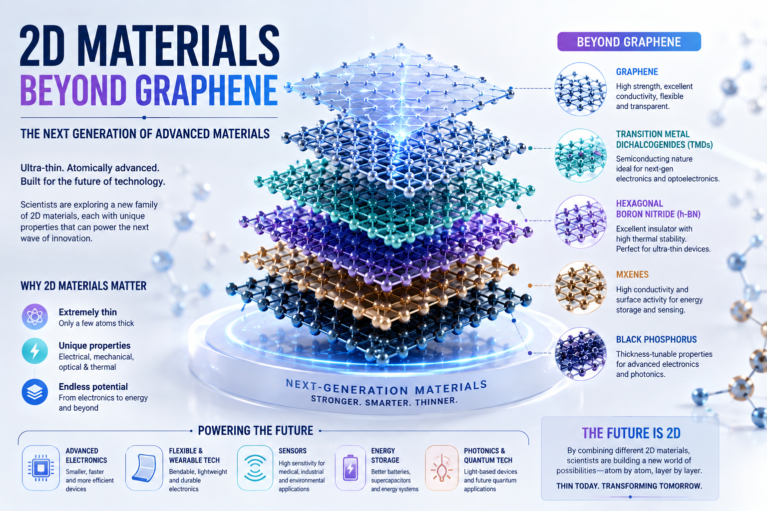
When people talk about advanced materials, graphene is often the first name that comes to mind. It is incredibly thin, strong, lightweight, and highly conductive.
But graphene is only the beginning.
Scientists and engineers are now exploring a much larger family of materials known as 2D materials. These materials are only a few atoms thick, yet they can have unusual electrical, mechanical, optical, and thermal properties.
From future computer chips and flexible electronics to sensors and energy storage, 2D materials beyond graphene could become an important part of next-generation technology.
What Are 2D Materials?
2D materials are materials that are extremely thin, sometimes only one or a few layers of atoms thick.
To understand how thin they are, imagine taking a normal material and continuing to peel it into thinner and thinner layers until only an atomic layer remains. That extremely thin layer can behave very differently from the original material.
This is what makes 2D materials so interesting.
At such a small scale, electrons and other physical properties can behave differently. As a result, these materials can offer useful characteristics for electronics, sensors, energy systems, and many other technologies.
Graphene is the most famous example, but there are many other 2D materials that scientists are studying.
Why Look Beyond Graphene?
Graphene has many impressive properties. It is strong, flexible, lightweight, and an excellent conductor of electricity and heat.
However, graphene is not perfect for every application.
One important limitation is that graphene does not naturally have the type of electronic bandgap that conventional semiconductor devices usually need. This can make it difficult to use graphene alone for certain types of transistors and digital electronics.
This is why researchers are looking beyond graphene.
Instead of trying to find one material that can do everything, scientists are developing different 2D materials for different jobs.
Some are better at controlling electricity. Others are useful as insulators, sensors, energy-storage materials, or optical components.
Transition Metal Dichalcogenides
One of the most interesting groups of 2D materials is called transition metal dichalcogenides, often shortened to TMDs.
Materials such as molybdenum disulfide (MoS₂) and tungsten diselenide (WSe₂) belong to this family.
What makes TMDs interesting is their semiconductor behavior. Because they can remain extremely thin while still providing useful electronic properties, researchers are studying them for future transistors, sensors, and optoelectronic devices.
For example, a very thin semiconductor could help engineers design smaller electronic components as traditional chip technology continues to become more compact.
Hexagonal Boron Nitride
Another important 2D material is hexagonal boron nitride, commonly known as h-BN.
It has a structure that looks similar to graphene, but its properties are quite different.
Unlike graphene, h-BN acts as an electrical insulator. This makes it useful as a supporting material in advanced electronic devices.
Researchers can combine h-BN with other 2D materials to create layered structures where each material performs a different function.
This idea is becoming an important part of modern 2D-material research.
MXenes
MXenes are another exciting family of 2D materials.
They are made from transition-metal compounds and have attracted attention because of their electrical conductivity and interesting surface properties.
Researchers are exploring MXenes for applications such as batteries, supercapacitors, sensors, electromagnetic shielding, and other advanced technologies.
One of their biggest advantages is that their surfaces can interact with different chemicals and materials. This gives engineers opportunities to modify them for specific applications.
Black Phosphorus
Black phosphorus is another 2D material that has attracted significant research interest.
One interesting feature of black phosphorus is that its electronic properties can change depending on how many atomic layers it contains.
This makes it potentially useful for electronics, sensors, and optical devices.
However, there is also a major challenge. Black phosphorus can degrade when exposed to environmental conditions such as oxygen and moisture.
So while it has exciting properties, researchers still need to solve its stability and manufacturing challenges before it can become widely used.
How 2D Materials Could Change Electronics
One of the biggest areas of interest for 2D materials is electronics and semiconductor technology.
Modern computer chips contain billions of tiny components, and engineers are constantly looking for ways to make these components smaller, faster, and more energy efficient.
Because 2D materials can be extremely thin, they could provide new options for building very small electronic devices.
Materials such as TMDs could potentially be used in future transistors and other semiconductor components.
However, this does not mean that 2D materials will simply replace silicon.
A more realistic future could involve 2D materials working together with silicon and other materials to create more advanced chips.
2D Materials and Flexible Electronics
Another exciting possibility is flexible electronics.
Traditional electronic components are usually built on rigid materials. But many 2D materials are naturally thin and flexible.
This could make them useful for technologies such as flexible displays, wearable devices, smart sensors, and electronic systems that can bend without losing their functionality.
Imagine electronic devices that can be placed on flexible surfaces or integrated into lightweight wearable products.
This is one area where the unique properties of 2D materials could become especially valuable.
2D Materials for Sensors
2D materials could also improve the way sensors detect things.
Because these materials have extremely thin structures and large surface areas relative to their thickness, their surfaces can interact strongly with surrounding substances.
This makes them interesting for chemical sensors, environmental monitoring, medical technologies, and industrial applications.
For example, researchers are investigating whether 2D materials can help sensors detect very small changes in gases, chemicals, temperature, pressure, or biological substances.
2D Materials and Energy Storage
The energy sector is another promising area.
Researchers are studying 2D materials for use in batteries, supercapacitors, solar technologies, and other energy systems.
Their large surface areas and electrical properties can potentially help improve how energy is stored or transferred.
MXenes, for example, are being studied extensively for energy-storage applications.
The goal is not necessarily to create a battery made entirely from one 2D material. Instead, these materials could become part of new battery designs that improve specific properties such as charging speed, energy storage, or durability.
Stacking Different 2D Materials
One of the most interesting ideas in this field is that engineers do not always need to choose just one material.
Different 2D materials can potentially be placed on top of each other to create a new structure.
These structures are sometimes called 2D heterostructures.
Think of it like building with very thin sheets. One sheet might conduct electricity, another might act as an insulator, and another might respond to light.
By combining them, engineers can create a system where each layer performs a specific job.
This could open the door to electronic and photonic devices with properties that are difficult to achieve using a single material.
What Are the Challenges?
2D materials have enormous potential, but they are not ready to solve every engineering problem yet.
One of the biggest challenges is manufacturing.
Producing a small sample of a high-quality 2D material in a laboratory is very different from producing millions of identical components for commercial products.
Researchers also need to deal with problems such as material defects, environmental stability, production costs, and integration with existing manufacturing processes.
For technologies such as computer chips, even very small differences between materials can affect performance.
Solving these manufacturing challenges will be critical before many 2D-material technologies can reach large-scale commercial use.
Are 2D Materials Going to Replace Graphene?
Probably not.
The future is unlikely to be about finding one material that simply replaces graphene.
Instead, different 2D materials will likely be used for different purposes.
Graphene can be useful when high electrical or thermal conductivity is needed. TMDs can provide useful semiconductor properties. h-BN can work as an insulating layer. MXenes may be valuable for energy storage and sensing.
The real opportunity is in combining these materials.
What Does the Future Look Like?
The development of 2D materials is still an active area of research, but the possibilities are exciting.
As manufacturing techniques improve, these materials could become part of future semiconductors, flexible electronics, sensors, batteries, photonic devices, and other advanced technologies.
The most important breakthrough may not come from discovering a single “super material.”
Instead, the future could come from learning how to combine different 2D materials and integrate them with technologies we already use.
Final Thoughts
Graphene showed the world that a material only one atom thick can have extraordinary properties.
Now, researchers are going much further.
From TMDs and h-BN to MXenes and black phosphorus, the world of 2D materials is expanding rapidly. Each material has its own strengths, weaknesses, and potential applications.
There are still major challenges to overcome, especially around large-scale manufacturing and reliability. But as engineers learn more about these materials, they could become an important part of the next generation of technology.
The future of advanced materials may not be about one material replacing another.
It may be about bringing many different materials together to build technologies that are smaller, smarter, lighter, and more efficient.
